https://dropithere.netlify.app/text/2YHoFbMDK1H3LDAKZCN3
http://ningspruz7.tech/button2901
An electronic amplifier, amplifier, or (informally) amp is an electronic device that increases the power of a signal. It does this by taking energy from a power supply and controlling the output to match the input signal shape but with a larger amplitude. In this sense, an amplifier modulates the output of the power supply.
There are four basic types of electronic amplifier: the voltage amplifier, the current amplifier, the transconductance amplifier, and the transresistance amplifier. A further distinction is whether the output is a linear or exponential representation of the input. As well, amplifiers can be categorized by their physical placement in the signal chain.[1]
Amplifier quality is characterized by a list of specifications that includes:
Amplifiers are described according to their input and output properties.[2] They have some kind of gain, or multiplication factor that relates the magnitude of the output signal to the input signal. The gain may be specified as the ratio of output voltage to input voltage (voltage gain), output power to input power (power gain), or some combination of current, voltage, and power. In many cases, with input and output in the same unit, gain is unitless (though often expressed in decibels).
The four basic types of amplifiers are as follows:[1]
The power gain of an amplifier depends on the source and load impedances used as well as its voltage gain; while an RF amplifier may have its impedances optimized for power transfer, audio and instrumentation amplifiers are normally employed with amplifier input and output impedances optimized for least loading and highest quality. So an amplifier that is said to have a gain of 20 dB might have a voltage gain of ten times and an available power gain of much more than 20 dB (100 times power ratio), yet be delivering a much lower power gain if, for example, the input is a 600 ohm microphone and the output is a 47 kilohm power amplifier's input socket.
In most cases an amplifier should be linear; that is, the gain should be constant for any combination of input and output signal. If the gain is not constant, e.g., by clipping the output signal at the limits of its capabilities, the output signal is distorted. There are however cases where variable gain is useful. Exponential gain amplifiers are used in certain signal processing applications.[1]
There are many types of electronic amplifiers, commonly used in radio and television transmitters and receivers, high-fidelity ("hi-fi") stereo equipment, microcomputers and other electronic digital equipment, and guitar and other instrument amplifiers. Critical components include active devices, such as vacuum tubes or transistors. A brief introduction to the many types of electronic amplifier follows.
The term power amplifier is a relative term with respect to the amount of power delivered to the load and/or sourced by the supply circuit. In general a power amplifier is designated as the last amplifier in a transmission chain (the output stage) and is the amplifier stage that typically requires most attention to power efficiency. Efficiency considerations lead to various classes of power amplifier based on the biasing of the output transistors or tubes: see power amplifier classes.
Power amplifier circuits include the following types:
According to Symons, while semiconductor amplifiers have largely displaced valve amplifiers for low power applications, valve amplifiers are much more cost effective in high power applications such as "radar, countermeasures equipment, or communications equipment" (p. 56). Many microwave amplifiers are specially designed valves, such as the klystron, gyrotron, traveling wave tube, and crossed-field amplifier, and these microwave valves provide much greater single-device power output at microwave frequencies than solid-state devices (p. 59).[4]
Valves/tube amplifiers also have niche uses in other areas, such as
The essential role of this active element is to magnify an input signal to yield a significantly larger output signal. The amount of magnification (the "forward gain") is determined by the external circuit design as well as the active device.
Many common active devices in transistor amplifiers are bipolar junction transistors (BJTs) and metal oxide semiconductor field-effect transistors (MOSFETs).
Applications are numerous, some common examples are audio amplifiers in a home stereo or PA system, RF high power generation for semiconductor equipment, to RF and Microwave applications such as radio transmitters.
Transistor-based amplifier can be realized using various configurations: for example with a bipolar junction transistor we can realize common base, common collector or common emitter amplifier; using a MOSFET we can realize common gate, common source or common drain amplifier. Each configuration has different characteristic (gain, impedance...).
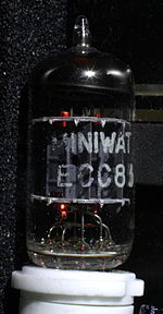
An operational amplifier is an amplifier circuit with very high open loop gain and differential inputs that employs external feedback to control its transfer function, or gain. Though the term today commonly applies to integrated circuits, the original operational amplifier design used valves.
A fully differential amplifier is a solid state integrated circuit amplifier that uses external feedback to control its transfer function or gain. It is similar to the operational amplifier, but also has differential output pins. These are usually constructed using BJTs or FETs.
These deal with video signals and have varying bandwidths depending on whether the video signal is for SDTV, EDTV, HDTV 720p or 1080i/p etc.. The specification of the bandwidth itself depends on what kind of filter is used—and at which point (-1 dB or -3 dB for example) the bandwidth is measured. Certain requirements for step response and overshoot are necessary for an acceptable TV image.
These deal with video signals that drive an oscilloscope display tube, and can have bandwidths of about 500 MHz. The specifications on step response, rise time, overshoot, and aberrations can make designing these amplifiers difficult. One of the pioneers in high bandwidth vertical amplifiers was the Tektronix company.
These use transmission lines to temporally split the signal and amplify each portion separately to achieve higher bandwidth than possible from a single amplifier. The outputs of each stage are combined in the output transmission line. This type of amplifier was commonly used on oscilloscopes as the final vertical amplifier. The transmission lines were often housed inside the display tube glass envelope.
These nonlinear amplifiers have much higher efficiencies than linear amps, and are used where the power saving justifies the extra complexity.
Negative resistances can be used as amplifiers, such as the tunnel diode amplifier.
Traveling wave tube amplifiers (TWTAs) are used for high power amplification at low microwave frequencies. They typically can amplify across a broad spectrum of frequencies; however, they are usually not as tunable as klystrons.
Klystrons are specialized linear-beam vacuum-devices, designed to provide high power, widely tunable amplification of millimetre and sub-millimetre waves. Klystrons are designed for large scale operations and despite having a narrower bandwidth than TWTAs, they have the advantage of coherently amplifying a reference signal so its output may be precisely controlled in amplitude, frequency and phase.
An audio power amplifier is usually used to amplify signals such as music or speech. Several factors are especially important in the selection of musical instrument amplifiers (such as guitar amplifiers) and other audio amplifiers (although the whole of the sound system – components such as microphones to loudspeakers – affect these parameters):
Many alternative classifications address different aspects of amplifier designs, and they all express some particular perspective relating the design parameters to the objectives of the circuit. Amplifier design is always a compromise of numerous factors, such as cost, power consumption, real-world device imperfections, and a multitude of performance specifications. Below are several different approaches to classification:
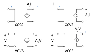
Electronic amplifiers use one variable presented as either a current and voltage. Either current or voltage can be used as input and either as output, leading to four types of amplifiers. In idealized form they are represented by each of the four types of dependent source used in linear analysis, as shown in the figure, namely:
Each type of amplifier in its ideal form has an ideal input and output resistance that is the same as that of the corresponding dependent source:[5]
In practice the ideal impedances are only approximated. For any particular circuit, a small-signal analysis is often used to find the impedance actually achieved. A small-signal AC test current Ix is applied to the input or output node, all external sources are set to AC zero, and the corresponding alternating voltage Vx across the test current source determines the impedance seen at that node as R = Vx / Ix.
Amplifiers designed to attach to a transmission line at input and/or output, especially RF amplifiers, do not fit into this classification approach. Rather than dealing with voltage or current individually, they ideally couple with an input and/or output impedance matched to the transmission line impedance, that is, match ratios of voltage to current. Many real RF amplifiers come close to this ideal. Although, for a given appropriate source and load impedance, RF amplifiers can be characterized as amplifying voltage or current, they fundamentally are amplifying power.[6]
One set of classifications for amplifiers is based on which device terminal is common to both the input and the output circuit. In the case of bipolar junction transistors, the three classes are common emitter, common base, and common collector. For field-effect transistors, the corresponding configurations are common source, common gate, and common drain; for triode vacuum devices, common cathode, common grid, and common plate. The output voltage of a common plate amplifier is the same as the input (this arrangement is used as the input presents a high impedance and does not load the signal source, although it does not amplify the voltage), i.e., the output at the cathode follows the input at the grid; consequently it was commonly called a cathode follower. By analogy the terms emitter follower and source follower are sometimes used.
When an amplifier has an output that exhibits no feedback to its input side, it is called 'unilateral'. The input impedance of a unilateral amplifier is independent of the load, and the output impedance is independent of the signal source impedance.
If feedback connects part of the output back to the input of the amplifier it is called a 'bilateral' amplifier. The input impedance of a bilateral amplifier is dependent upon the load, and the output impedance is dependent upon the signal source impedance.
All amplifiers are bilateral to some degree; however they may often be modeled as unilateral under operating conditions where feedback is small enough to neglect for most purposes, simplifying analysis (see the common base article for an example).
Negative feedback is often applied deliberately to tailor amplifier behavior. Some feedback, which may be positive or negative, is unavoidable and often undesirable, introduced, for example, by parasitic elements such as the inherent capacitance between input and output of a device such as a transistor and capacitative coupling due to external wiring. Excessive frequency-dependent positive feedback may cause what is intended/expected to be an amplifier to become an oscillator.
Linear unilateral and bilateral amplifiers can be represented as two-port networks.
Another way to classify amps is the phase relationship of the input signal to the output signal. An 'inverting' amplifier produces an output 180 degrees out of phase with the input signal (that is, a polarity inversion or mirror image of the input as seen on an oscilloscope). A 'non-inverting' amplifier maintains the phase of the input signal waveforms. An emitter follower is a type of non-inverting amplifier, indicating that the signal at the emitter of a transistor is following (that is, matching with unity gain but perhaps an offset) the input signal.
This description can apply to a single stage of an amplifier, or to a complete amplifier system.
Other amplifiers may be classified by their function or output characteristics. These functional descriptions usually apply to complete amplifier systems or sub-systems and rarely to individual stages.
The performance of an op-amp with these characteristics is entirely defined by the (usually passive) components that form a negative feedback loop around it. The amplifier itself does not effect the output. All real-world op-amps fall short of the idealised specification above—but some modern components have remarkable performance and come close in some respects.
Amplifiers are sometimes classified by the coupling method of the signal at the input, output, or between stages. Different types of these include:
Depending on the frequency range and other properties amplifiers are designed according to different principles.
The frequency range handled by an amplifier might be specified in terms of bandwidth (normally implying a response that is 3 dB down when the frequency reaches the specified bandwidth), or by specifying a frequency response that is within a certain number of decibels between a lower and an upper frequency (e.g. "20 Hz to 20 kHz plus or minus 1 dB").
Power amplifier circuits (output stages) are classified as A, B, AB and C for analog designs, and class D and E for switching designs based on the proportion of each input cycle (conduction angle), during which an amplifying device is passing current. The image of the conduction angle is derived from amplifying a sinusoidal signal. If the device is always on, the conducting angle is 360°. If it is on for only half of each cycle, the angle is 180°. The angle of flow is closely related to the amplifier power efficiency. The various classes are introduced below, followed by a more detailed discussion under their individual headings further down.
In the illustrations below, a bipolar junction transistor is shown as the amplifying device, but the same attributes are found if with MOSFETs or vacuum tubes.
A "Class D" amplifier uses some form of pulse-width modulation to control the output devices; the conduction angle of each device is no longer related directly to the input signal but instead varies in pulse width. These are sometimes called "digital" amplifiers because the output device is switched fully on or off, and not carrying current proportional to the signal amplitude.
Amplifying devices operating in class A conduct over the whole of the input cycle. A class-A amplifier is distinguished by the output stage being biased into class A (see definition above). Subclass A2 is sometimes used to refer to vacuum-tube class-A stages where the grid is allowed to be driven slightly positive on signal peaks, resulting in slightly more power than normal class A (A1; where the grid is always negative[9]), but incurring more distortion.
Class-A designs have largely been superseded by the more efficient designs for power amplifiers, though they remain popular with some hobbyists, mostly for their simplicity. There is a market for expensive high fidelity class-A amps considered a "cult item" amongst audiophiles[10] mainly for their absence of crossover distortion and reduced odd-harmonic and high-order harmonic distortion.
Some aficionados[who?] who prefer class-A amplifiers also prefer the use of thermionic valve (or "tube") designs instead of transistors, especially in Single-ended triode output configurations for several claimed reasons:
Transistors are much cheaper, and so more elaborate designs that give greater efficiency but use more parts are still cost-effective. A classic application for a pair of class-A devices is the long-tailed pair, which is exceptionally linear, and forms the basis of many more complex circuits, including many audio amplifiers and almost all op-amps.
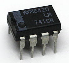
Class-A amplifiers are often used in output stages of high quality op-amps[citation needed] (although the accuracy of the bias in low cost op-amps such as the 741 may result in class A or class AB or class B, varying from device to device or with temperature). They are sometimes used as medium-power, low-efficiency, and high-cost audio power amplifiers. The power consumption is unrelated to the output power. At idle (no input), the power consumption is essentially the same as at high output volume. The result is low efficiency and high heat dissipation.
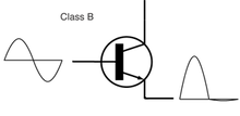
Class-B amplifiers only amplify half of the input wave cycle, thus creating a large amount of distortion, but their efficiency is greatly improved and is much better than class A. Class-B amplifiers are also favoured in battery-operated devices, such as transistor radios. Class B has a maximum theoretical efficiency of π/4. (i.e. 78.5%) This is because the amplifying element is switched off altogether half of the time, and so cannot dissipate power. A single class-B element is rarely found in practice, though it has been used for driving the loudspeaker in the early IBM Personal Computers with beeps, and it can be used in RF power amplifier where the distortion levels are less important. However, class C is more commonly used for this.
A practical circuit using class-B elements is the push–pull stage, such as the very simplified complementary pair arrangement shown below. Here, complementary or quasi-complementary devices are each used for amplifying the opposite halves of the input signal, which is then recombined at the output. This arrangement gives excellent efficiency, but can suffer from the drawback that there is a small mismatch in the cross-over region – at the "joins" between the two halves of the signal, as one output device has to take over supplying power exactly as the other finishes. This is called crossover distortion. An improvement is to bias the devices so they are not completely off when they're not in use. This approach is called class AB operation.
Class AB is widely considered a good compromise for audio power amplifiers, since much of the time the music is quiet enough that the signal stays in the "class A" region, where it is amplified with good fidelity, and by definition if passing out of this region, is large enough that the distortion products typical of class B are relatively small. The crossover distortion can be reduced further by using negative feedback.
In class-AB operation, each device operates the same way as in class B over half the waveform, but also conducts a small amount on the other half. As a result, the region where both devices simultaneously are nearly off (the "dead zone") is reduced. The result is that when the waveforms from the two devices are combined, the crossover is greatly minimised or eliminated altogether. The exact choice of quiescent current, the standing current through both devices when there is no signal, makes a large difference to the level of distortion (and to the risk of thermal runaway, that may damage the devices); often the bias voltage applied to set this quiescent current has to be adjusted with the temperature of the output transistors (for example in the circuit at the beginning of the article the diodes would be mounted physically close to the output transistors, and chosen to have a matched temperature coefficient). Another approach (often used as well as thermally tracking bias voltages) is to include small value resistors in series with the emitters.
Class AB sacrifices some efficiency over class B in favor of linearity, thus is less efficient (below 78.5% for full-amplitude sinewaves in transistor amplifiers, typically; much less is common in class-AB vacuum-tube amplifiers). It is typically much more efficient than class A.
Sometimes a numeral is added for vacuum-tube stages. If the grid voltage is always negative with respect to the cathode the class is AB1. If the grid is allowed to go slightly positive (hence drawing grid current, adding more distortion, but giving slightly higher output power) on signal peaks the class is AB2.
Class-C amplifiers conduct less than 50% of the input signal and the distortion at the output is high, but high efficiencies (up to 90%) are possible. The usual application for class-C amplifiers is in RF transmitters operating at a single fixed carrier frequency, where the distortion is controlled by a tuned load on the amplifier. The input signal is used to switch the active device causing pulses of current to flow through a tuned circuit forming part of the load.
The class-C amplifier has two modes of operation: tuned and untuned.[13] The diagram shows a waveform from a simple class-C circuit without the tuned load. This is called untuned operation, and the analysis of the waveforms shows the massive distortion that appears in the signal. When the proper load (e.g., an inductive-capacitive filter plus a load resistor) is used, two things happen. The first is that the output's bias level is clamped with the average output voltage equal to the supply voltage. This is why tuned operation is sometimes called a clamper. This allows the waveform to be restored to its proper shape despite the amplifier having only a one-polarity supply. This is directly related to the second phenomenon: the waveform on the center frequency becomes less distorted. The residual distortion is dependent upon the bandwidth of the tuned load, with the center frequency seeing very little distortion, but greater attenuation the farther from the tuned frequency that the signal gets.
The tuned circuit resonates at one frequency, the fixed carrier frequency, and so the unwanted frequencies are suppressed, and the wanted full signal (sine wave) is extracted by the tuned load. The signal bandwidth of the amplifier is limited by the Q-factor of the tuned circuit but this is not a serious limitation. Any residual harmonics can be removed using a further filter.
In practical class-C amplifiers a tuned load is invariably used. In one common arrangement the resistor shown in the circuit above is replaced with a parallel-tuned circuit consisting of an inductor and capacitor in parallel, whose components are chosen to resonate the frequency of the input signal. Power can be coupled to a load by transformer action with a secondary coil wound on the inductor. The average voltage at the drain is then equal to the supply voltage, and the signal voltage appearing across the tuned circuit varies from near zero to near twice the supply voltage during the rf cycle. The input circuit is biassed so that the active element (e.g. transistor) conducts for only a fraction of the rf cycle, usually one third (120 degrees) or less.[14]
The active element conducts only while the drain voltage is passing through its minimum. By this means, power dissipation in the active device is minimised, and efficiency increased. Ideally, the active element would pass only an instantaneous current pulse while the voltage across it is zero: it then dissipates no power and 100% efficiency is achieved. However practical devices have a limit to the peak current they can pass, and the pulse must therefore be widened, to around 120 degrees, to obtain a reasonable amount of power, and the efficiency is then 60-70%.[14]
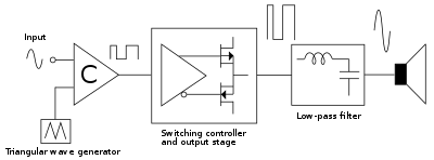
In the class-D amplifier the input signal is converted to a sequence of higher voltage output pulses. The averaged-over-time power values of these pulses are directly proportional to the instantaneous amplitude of the input signal. The frequency of the output pulses is typically ten or more times the highest frequency in the input signal to be amplified. The output pulses contain inaccurate spectral components (that is, the pulse frequency and its harmonics), which must be removed by a low-pass passive filter. The resulting filtered signal is then an amplified replica of the input.
These amplifiers use pulse width modulation, pulse density modulation (sometimes referred to as pulse frequency modulation) or a more advanced form of modulation such as Delta-sigma modulation (for example, in the Analog Devices AD1990 class-D audio power amplifier). Output stages such as those used in pulse generators are examples of class-D amplifiers. The term class D is usually applied to devices intended to reproduce signals with a bandwidth well below the switching frequency.
Class-D amplifiers can be controlled by either analog or digital circuits. The digital control introduces additional distortion called quantization error caused by its conversion of the input signal to a digital value.
The main advantage of a class-D amplifier is power efficiency. Because the output pulses have a fixed amplitude, the switching elements (usually MOSFETs, but valves (vacuum tubes) and bipolar transistors were once used) are switched either completely on or completely off, rather than operated in linear mode. A MOSFET operates with the lowest resistance when fully on and thus (excluding when fully off) has the lowest power dissipation when in that condition. Compared to an equivalent class-AB device, a class-D amplifier's lower losses permit the use of a smaller heat sink for the MOSFETs while also reducing the amount of input power required, allowing for a lower-capacity power supply design. Therefore, class-D amplifiers are typically smaller than an equivalent class-AB amplifier.
Class-D amplifiers have been widely used to control motors, but they are now also used as audio power amplifiers, with some extra circuitry to allow analogue to be converted to a much higher frequency pulse width modulated signal.
High quality class-D audio power amplifiers have now appeared on the market. These designs have been said to rival traditional AB amplifiers in terms of quality. An early use of class-D amplifiers was high-power subwoofer amplifiers in cars. Because subwoofers are generally limited to a bandwidth of no higher than 150 Hz, the switching speed for the amplifier does not have to be as high as for a full range amplifier, allowing simpler designs. Class-D amplifiers for driving subwoofers are relatively inexpensive in comparison to class-AB amplifiers.
The letter D used to designate this amplifier class is simply the next letter after C, and does not stand for digital. Class-D and class-E amplifiers are sometimes mistakenly described as "digital" because the output waveform superficially resembles a pulse-train of digital symbols, but a class-D amplifier merely converts an input waveform into a continuously pulse-width modulated (square wave) analog signal. (A digital waveform would be pulse-code modulated.)
The class-E/F amplifier is a highly efficient switching power amplifier, typically used at such high frequencies that the switching time becomes comparable to the duty time. As said in the class-D amplifier, the transistor is connected via a serial LC circuit to the load, and connected via a large L (inductor) to the supply voltage. The supply voltage is connected to ground via a large capacitor to prevent any RF signals leaking into the supply. The class-E amplifier adds a C (capacitor) between the transistor and ground and uses a defined L1 to connect to the supply voltage.
The following description ignores DC, which can be added easily afterwards. The above mentioned C and L are in effect a parallel LC circuit to ground. When the transistor is on, it pushes through the serial LC circuit into the load and some current begins to flow to the parallel LC circuit to ground. Then the serial LC circuit swings back and compensates the current into the parallel LC circuit. At this point the current through the transistor is zero and it is switched off. Both LC circuits are now filled with energy in C and L0. The whole circuit performs a damped oscillation. The damping by the load has been adjusted so that some time later the energy from the Ls is gone into the load, but the energy in both C0 peaks at the original value to in turn restore the original voltage so that the voltage across the transistor is zero again and it can be switched on.
With load, frequency, and duty cycle (0.5) as given parameters and the constraint that the voltage is not only restored, but peaks at the original voltage, the four parameters (L, L0, C and C0) are determined. The class-E amplifier takes the finite on resistance into account and tries to make the current touch the bottom at zero. This means that the voltage and the current at the transistor are symmetric with respect to time. The Fourier transform allows an elegant formulation to generate the complicated LC networks and says that the first harmonic is passed into the load, all even harmonics are shorted and all higher odd harmonics are open.
Class E uses a significant amount of second-harmonic voltage. The second harmonic can be used to reduce the overlap with edges with finite sharpness. For this to work, energy on the second harmonic has to flow from the load into the transistor, and no source for this is visible in the circuit diagram. In reality, the impedance is mostly reactive and the only reason for it is that class E is a class F (see below) amplifier with a much simplified load network and thus has to deal with imperfections.
In many amateur simulations of class-E amplifiers, sharp current edges are assumed nullifying the very motivation for class E and measurements near the transit frequency of the transistors show very symmetric curves, which look much similar to class-F simulations.
The class-E amplifier was invented in 1972 by Nathan O. Sokal and Alan D. Sokal, and details were first published in 1975.[15] Some earlier reports on this operating class have been published in Russian.
In push–pull amplifiers and in CMOS, the even harmonics of both transistors just cancel. Experiment shows that a square wave can be generated by those amplifiers. Theoretically square waves consist of odd harmonics only. In a class-D amplifier, the output filter blocks all harmonics; i.e., the harmonics see an open load. So even small currents in the harmonics suffice to generate a voltage square wave. The current is in phase with the voltage applied to the filter, but the voltage across the transistors is out of phase. Therefore, there is a minimal overlap between current through the transistors and voltage across the transistors. The sharper the edges, the lower the overlap.
While in class D, transistors and the load exist as two separate modules, class F admits imperfections like the parasitics of the transistor and tries to optimise the global system to have a high impedance at the harmonics. Of course there has to be a finite voltage across the transistor to push the current across the on-state resistance. Because the combined current through both transistors is mostly in the first harmonic, it looks like a sine. That means that in the middle of the square the maximum of current has to flow, so it may make sense to have a dip in the square or in other words to allow some overswing of the voltage square wave. A class-F load network by definition has to transmit below a cutoff frequency and reflect above.
Any frequency lying below the cutoff and having its second harmonic above the cutoff can be amplified, that is an octave bandwidth. On the other hand, an inductive-capacitive series circuit with a large inductance and a tunable capacitance may be simpler to implement. By reducing the duty cycle below 0.5, the output amplitude can be modulated. The voltage square waveform degrades, but any overheating is compensated by the lower overall power flowing. Any load mismatch behind the filter can only act on the first harmonic current waveform, clearly only a purely resistive load makes sense, then the lower the resistance, the higher the current.
Class F can be driven by sine or by a square wave, for a sine the input can be tuned by an inductor to increase gain. If class F is implemented with a single transistor, the filter is complicated to short the even harmonics. All previous designs use sharp edges to minimise the overlap.
There are a variety of amplifier designs that enhance class-AB output stages with more efficient techniques to achieve greater efficiencies with low distortion. These designs are common in large audio amplifiers since the heatsinks and power transformers would be prohibitively large (and costly) without the efficiency increases. The terms "class G" and "class H" are used interchangeably to refer to different designs, varying in definition from one manufacturer or paper to another.
Class-G amplifiers (which use "rail switching" to decrease power consumption and increase efficiency) are more efficient than class-AB amplifiers. These amplifiers provide several power rails at different voltages and switch between them as the signal output approaches each level. Thus, the amplifier increases efficiency by reducing the wasted power at the output transistors. Class-G amplifiers are more efficient than class AB but less efficient when compared to class D, without the negative EMI effects of class D.
Class-H amplifiers take the idea of class G one step further creating an infinitely variable supply rail. This is done by modulating the supply rails so that the rails are only a few volts larger than the output signal at any given time. The output stage operates at its maximum efficiency all the time. Switched-mode power supplies can be used to create the tracking rails. Significant efficiency gains can be achieved but with the drawback of more complicated supply design and reduced THD performance. In common designs, a voltage drop of about 10V is maintained over the output transistors in Class H circuits. The picture above shows positive supply voltage of the output stage and the voltage at the speaker output. The boost of the supply voltage is shown for a real music signal.
The voltage signal shown is thus a larger version of the input, but has been changed in sign (inverted) by the amplification. Other arrangements of amplifying device are possible, but that given (that is, common emitter, common source or common cathode) is the easiest to understand and employ in practice. If the amplifying element is linear, the output is a faithful copy of the input, only larger and inverted. In practice, transistors are not linear, and the output only approximates the input. nonlinearity from any of several sources is the origin of distortion within an amplifier. The class of amplifier (A, B, AB or C) depends on how the amplifying device is biased. The diagrams omit the bias circuits for clarity.
Any real amplifier is an imperfect realization of an ideal amplifier. An important limitation of a real amplifier is that the output it generates is ultimately limited by the power available from the power supply. An amplifier saturates and clips the output if the input signal becomes too large for the amplifier to reproduce or exceeds operational limits for the device.
The Doherty, a hybrid configuration, is receiving new attention. It was invented in 1934 by William H. Doherty for Bell Laboratories—whose sister company, Western Electric, manufactured radio transmitters. The Doherty amplifier consists of a class-B primary or carrier stages in parallel with a class-C auxiliary or peak stage. The input signal splits to drive the two amplifiers, and a combining network sums the two output signals. Phase shifting networks are used in inputs and outputs. During periods of low signal level, the class-B amplifier efficiently operates on the signal and the class-C amplifier is cutoff and consumes little power. During periods of high signal level, the class-B amplifier delivers its maximum power and the class-C amplifier delivers up to its maximum power. The efficiency of previous AM transmitter designs was proportional to modulation but, with average modulation typically around 20%, transmitters were limited to less than 50% efficiency. In Doherty's design, even with zero modulation, a transmitter could achieve at least 60% efficiency.[16]
As a successor to Western Electric for broadcast transmitters, the Doherty concept was considerably refined by Continental Electronics Manufacturing Company of Dallas, TX. Perhaps, the ultimate refinement was the screen-grid modulation scheme invented by Joseph B. Sainton. The Sainton amplifier consists of a class-C primary or carrier stage in parallel with a class-C auxiliary or peak stage. The stages are split and combined through 90-degree phase shifting networks as in the Doherty amplifier. The unmodulated radio frequency carrier is applied to the control grids of both tubes. Carrier modulation is applied to the screen grids of both tubes. The bias point of the carrier and peak tubes is different, and is established such that the peak tube is cutoff when modulation is absent (and the amplifier is producing rated unmodulated carrier power) whereas both tubes contribute twice the rated carrier power during 100% modulation (as four times the carrier power is required to achieve 100% modulation). As both tubes operate in class C, a significant improvement in efficiency is thereby achieved in the final stage. In addition, as the tetrode carrier and peak tubes require very little drive power, a significant improvement in efficiency within the driver stage is achieved as well (317C, et al.).[17] The released version of the Sainton amplifier employs a cathode-follower modulator, not a push–pull modulator. Previous Continental Electronics designs, by James O. Weldon and others, retained most of the characteristics of the Doherty amplifier but added screen-grid modulation of the driver (317B, et al.).
The Doherty amplifier remains in use in very-high-power AM transmitters, but for lower-power AM transmitters, vacuum-tube amplifiers in general were eclipsed in the 1980s by arrays of solid-state amplifiers, which could be switched on and off with much finer granularity in response to the requirements of the input audio. However, interest in the Doherty configuration has been revived by cellular-telephone and wireless-Internet applications where the sum of several constant envelope users creates an aggregate AM result. The main challenge of the Doherty amplifier for digital transmission modes is in aligning the two stages and getting the class-C amplifier to turn on and off very quickly.
Recently, Doherty amplifiers have found widespread use in cellular base station transmitters for GHz frequencies. Implementations for transmitters in mobile devices have also been demonstrated.
Amplifiers are implemented using active elements of different kinds:
For special purposes, other active elements have been used. For example, in the early days of the satellite communication, parametric amplifiers were used. The core circuit was a diode whose capacity was changed by an RF signal created locally. Under certain conditions, this RF signal provided energy that was modulated by the extremely weak satellite signal received at the earth station.
The practical amplifier circuit to the right could be the basis for a moderate-power audio amplifier. It features a typical (though substantially simplified) design as found in modern amplifiers, with a class-AB push–pull output stage, and uses some overall negative feedback. Bipolar transistors are shown, but this design would also be realizable with FETs or valves.
The input signal is coupled through capacitor C1 to the base of transistor Q1. The capacitor allows the AC signal to pass, but blocks the DC bias voltage established by resistors R1 and R2 so that any preceding circuit is not affected by it. Q1 and Q2 form a differential amplifier (an amplifier that multiplies the difference between two inputs by some constant), in an arrangement known as a long-tailed pair. This arrangement is used to conveniently allow the use of negative feedback, which is fed from the output to Q2 via R7 and R8.
The negative feedback into the difference amplifier allows the amplifier to compare the input to the actual output. The amplified signal from Q1 is directly fed to the second stage, Q3, which is a common emitter stage that provides further amplification of the signal and the DC bias for the output stages, Q4 and Q5. R6 provides the load for Q3 (A better design would probably use some form of active load here, such as a constant-current sink). So far, all of the amplifier is operating in class A. The output pair are arranged in class-AB push–pull, also called a complementary pair. They provide the majority of the current amplification (while consuming low quiescent current) and directly drive the load, connected via DC-blocking capacitor C2. The diodes D1 and D2 provide a small amount of constant voltage bias for the output pair, just biasing them into the conducting state so that crossover distortion is minimized. That is, the diodes push the output stage firmly into class-AB mode (assuming that the base-emitter drop of the output transistors is reduced by heat dissipation).
This design is simple, but a good basis for a practical design because it automatically stabilises its operating point, since feedback internally operates from DC up through the audio range and beyond. Further circuit elements would probably be found in a real design that would roll off the frequency response above the needed range to prevent the possibility of unwanted oscillation. Also, the use of fixed diode bias as shown here can cause problems if the diodes are not both electrically and thermally matched to the output transistors – if the output transistors turn on too much, they can easily overheat and destroy themselves, as the full current from the power supply is not limited at this stage.
A common solution to help stabilise the output devices is to include some emitter resistors, typically an ohm or so. Calculating the values of the circuit's resistors and capacitors is done based on the components employed and the intended use of the amp.
For the basics of radio frequency amplifiers using valves, see Valved RF amplifiers.
Real world amplifiers are imperfect.
Different methods of supplying power result in many different methods of bias. Bias is a technique by which the active devices are set up to operate in a particular region, or by which the DC component of the output signal is set to the midpoint between the maximum voltages available from the power supply. Most amplifiers use several devices at each stage; they are typically matched in specifications except for polarity. Matched inverted polarity devices are called complementary pairs. Class-A amplifiers generally use only one device, unless the power supply is set to provide both positive and negative voltages, in which case a dual device symmetrical design may be used. Class-C amplifiers, by definition, use a single polarity supply.
Amplifiers often have multiple stages in cascade to increase gain. Each stage of these designs may be a different type of amp to suit the needs of that stage. For instance, the first stage might be a class-A stage, feeding a class-AB push–pull second stage, which then drives a class-G final output stage, taking advantage of the strengths of each type, while minimizing their weaknesses.
This website is powered by Spruz